- 您现在的位置:买卖IC网 > Sheet目录2008 > MAX1434ECQ+D (Maxim Integrated Products)IC ADC 10BIT 50MSPS 100-TQFP
then presented to the first-stage quantizers and isolate
the pipelines from the fast-changing inputs. Analog
inputs, IN_P to IN_N, are driven differentially. For differ-
ential inputs, balance the input impedance of IN_P and
IN_N for optimum performance.
Reference Configurations (REFIO,
REFADJ, REFP, and REFN)
The MAX1434 provides an internal 1.24V bandgap ref-
erence or can be driven with an external reference volt-
age. The full-scale analog differential input range is
±FSR. FSR (full-scale range) is given by the following
equation:
where VREFIO is the voltage at REFIO, generated inter-
nally or externally. For a VREFIO = 1.24V, the full-scale
input range is ±700mV (1.4VP-P).
Internal Reference Mode
Connect REFADJ to GND to use the internal bandgap
reference directly. The internal bandgap reference gen-
erates VREFIO to be 1.24V with a 120ppm/°C tempera-
ture coefficient in internal reference mode. Connect an
external
≥ 0.1F bypass capacitor from REFIO to GND
for stability. REFIO sources up to 200A and sinks up
to 200A for external circuits, and REFIO has a
75mV/mA load regulation. REFIO has > 1M
to GND
when the MAX1434 is in power-down mode. The inter-
nal reference circuit requires 100ms (CREFP to GND =
CREFN to GND = 1F) to power up and settle when
power is applied to the MAX1434 or when PD transi-
tions from high to low.
To compensate for gain errors or to decrease or
increase the ADC’s FSR, add an external resistor
between REFADJ and GND or REFADJ and REFIO.
This adjusts the internal reference value of the
MAX1434 by up to ±5% of its nominal value. See the
Full-Scale Range Adjustments Using the Internal
Reference section.
FSR
V
REFIO
=
×
(.
)
.
0 700
124
MAX1434
Octal, 10-Bit, 50Msps, 1.8V ADC
with Serial LVDS Outputs
______________________________________________________________________________________________________
13
MAX1434
IN_P
IN_N
OTA
AVDD
GND
C2a
S4b
S4c
S1
C2b
S4a
C1a
S2a
S5a
S3a
S3b
S5b
C1b
S2b
INTERNAL
BIAS*
OUT
INTERNALLY
GENERATED
COMMON-MODE
LEVEL*
SWITCHES SHOWN IN TRACK MODE
INTERNALLY
GENERATED
COMMON-MODE
LEVEL*
INTERNAL
COMMON-MODE
BIAS*
INTERNAL
COMMON-MODE
BIAS*
*NOT EXTERNALLY ACCESSIBLE
INTERNAL
BIAS*
OUT
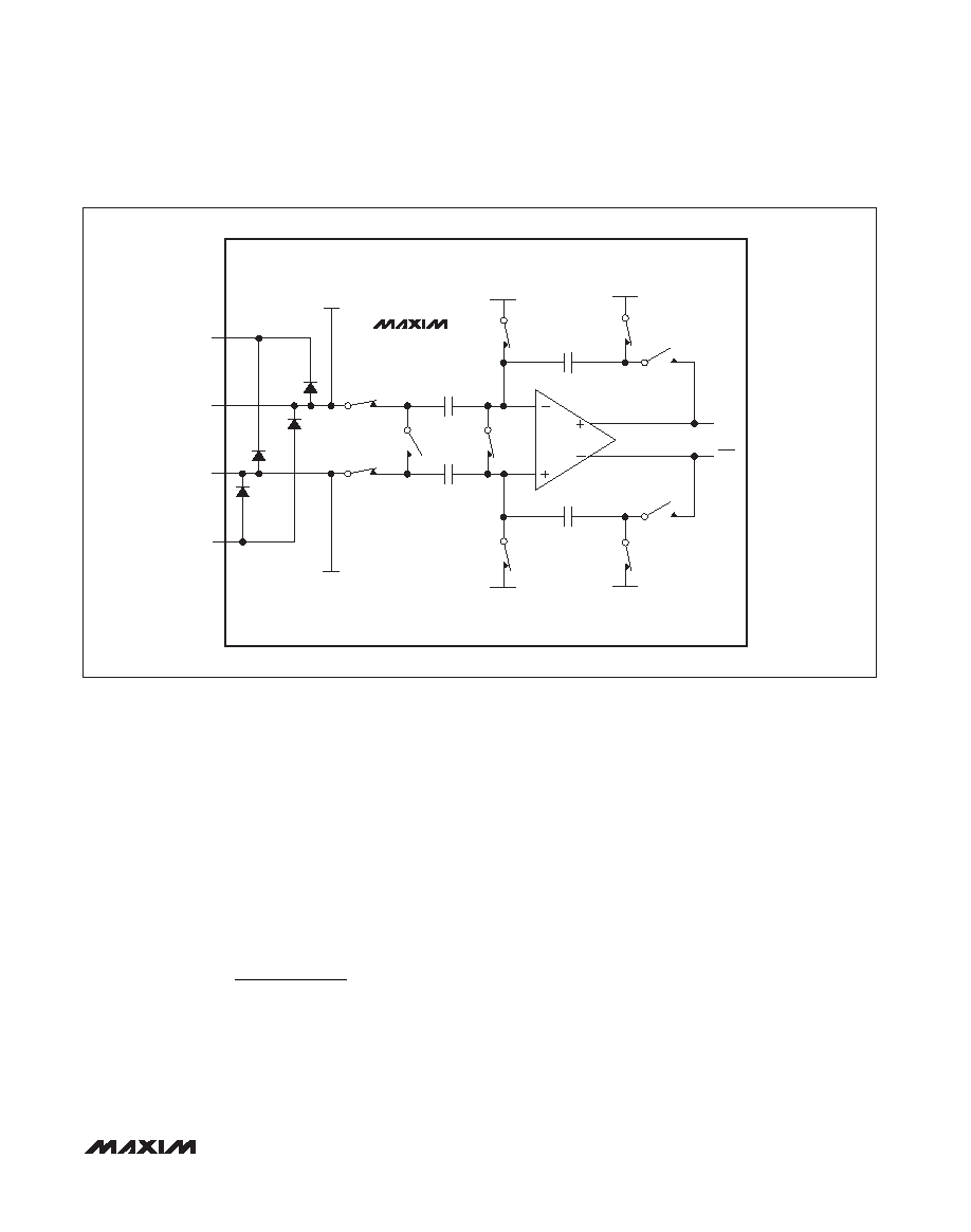
Figure 1. Internal Input Circuit
发布紧急采购,3分钟左右您将得到回复。
相关PDF资料
MAX1444EHJ+T
IC ADC 10BIT 40MSPS 32-TQFP
MAX1499ECJ+
IC ADC 3 1/2DIG W/LED DVR 32TQFP
MAX152EPP+
IC ADC 8BIT 1UA PWR-DWN 20-DIP
MAX153EPP+
IC ADC 8BIT 1MSPS HI-SPD 20-DIP
MAX154AENG+
IC ADC 8BIT 4CH W/MUX&REF 24-DIP
MAX155AEPI+
IC ADC 8BIT 8CH T/H&REF 28-DIP
MAX157AEUA+
IC ADC 10BIT 108KSPS 2CH 8-UMAX
MAX160CPN+
IC ADC 8BIT UP COMPATIBLE 18-DIP
相关代理商/技术参数
MAX1434ECQ+TD
功能描述:模数转换器 - ADC 10-Bit 8Ch 50Msps 1.8V High Speed ADC RoHS:否 制造商:Texas Instruments 通道数量:2 结构:Sigma-Delta 转换速率:125 SPs to 8 KSPs 分辨率:24 bit 输入类型:Differential 信噪比:107 dB 接口类型:SPI 工作电源电压:1.7 V to 3.6 V, 2.7 V to 5.25 V 最大工作温度:+ 85 C 安装风格:SMD/SMT 封装 / 箱体:VQFN-32
MAX1434ECQ-D
功能描述:模数转换器 - ADC RoHS:否 制造商:Texas Instruments 通道数量:2 结构:Sigma-Delta 转换速率:125 SPs to 8 KSPs 分辨率:24 bit 输入类型:Differential 信噪比:107 dB 接口类型:SPI 工作电源电压:1.7 V to 3.6 V, 2.7 V to 5.25 V 最大工作温度:+ 85 C 安装风格:SMD/SMT 封装 / 箱体:VQFN-32
MAX1434ECQ-TD
功能描述:模数转换器 - ADC RoHS:否 制造商:Texas Instruments 通道数量:2 结构:Sigma-Delta 转换速率:125 SPs to 8 KSPs 分辨率:24 bit 输入类型:Differential 信噪比:107 dB 接口类型:SPI 工作电源电压:1.7 V to 3.6 V, 2.7 V to 5.25 V 最大工作温度:+ 85 C 安装风格:SMD/SMT 封装 / 箱体:VQFN-32
MAX1434EVKIT
功能描述:数据转换 IC 开发工具 Evaluation Kit for the MAX1434 MAX1436 MAX1437 MAX1438 RoHS:否 制造商:Texas Instruments 产品:Demonstration Kits 类型:ADC 工具用于评估:ADS130E08 接口类型:SPI 工作电源电压:- 6 V to + 6 V
MAX1436BECQ
制造商:Rochester Electronics LLC 功能描述: 制造商:Maxim Integrated Products 功能描述:
MAX1436BECQ+D
制造商:Maxim Integrated Products 功能描述:ADC OCTAL PIPELINED 40MSPS 12-BIT SERL - Rail/Tube
MAX1436BECQ+TD
制造商:Maxim Integrated Products 功能描述:OCTAL 12BIT 40MSPS ADC - Tape and Reel
MAX1436ECQ
制造商:Rochester Electronics LLC 功能描述: 制造商:Maxim Integrated Products 功能描述: